PSoC 4xxx series
Category families This page contains information about the Infineon PSoC 4xxx series. TOC
Connection behavior
The connect sequence of PSoC 4 devices is very time critical and is thus performed from the J-Link/Flasher side directly.
When connecting to a PSoC 4 device that is in protected state, direct access to the internal flash contents is not possible.
When using J-Link / J-Flash, a connection to a device in protected state automatically triggers the sequence required to return the device to open state. Changing the protection level from protected to open requires a mass erase of the device. Consequently, the internal flash contents are erased as part of this operation.
Simply attempting to read a protected PSoC 4 device does not inherently require the device to be erased. The automatic mass-erase behavior described above is specific to the J-Link / J-Flash handling of protected devices.
Readout protection
The following section explains how to set Infineon PSoC 4 devices in protected state and how to unprotect them.
- The Infineon CY8C4xxx and CYBLExxxx series devices provide chip-level protection which allows permanent and non-permanent protection of the device concerning read and write access.
- The sequence, to secure the device consists of multiple read / write accesses to special function registers of the CY8C4xxx and CYBLExxxx series devices.
- PSoC4100/4200 target devices use different addresses for the SYSREQ and SYSARG registers. They are located at 0x40000004 and 0x40000008 instead. For more information please consult the Infineon Programming Specifications user guide.
- The clock of some PSoC4 target devices must be set to 48MHz before calling the locking/unlocking sequence. This can be achieved by using the "Configure Clock" Command. Please refer to the Infineon Programming specification for the related devices for information about which targets do require the sequence.
Changing protection - pseudo code
//
// Addresses
//
if (PSOC4000) {                   // PSOC4000: CPUSS base is 0x4010_0000
  CPUSS_BASE              = 0x40100000;
} else {                          // Other:    CPUSS base is 0x4000_0000
  CPUSS_BASE              = 0x40000000;
}
CPUSS_SYSREQ              = CPUSS_BASE + 0x04;
CPUSS_SYSARG              = CPUSS_BASE + 0x08;
//
// Register bits
//
CPUSS_SYSREQ_BIT          = (1 << 31);
CPUSS_CMD_SHIFT           = 0;
//
// SROM constants
//
SROM_KEY1                 = 0xB6;
SROM_KEY2                 = 0xD3;
//
// SROM requests
//
SROM_CMD_WRITE_PROTECTION = 0x0D; // Write chip-level (and flash) protection.
SROM_CMD_SET_IMO_48MHz    = 0x15; // Set clock to 48 MHz (req. for flash programming)
//
// Chip protection levels
//
CHIP_PROT_OPEN            = 0x01; // OPEN (unprotected)
CHIP_PROT_PROTECTED       = 0x02; // PROTECTED (chip protected, reversible)
CHIP_PROT_KILL            = 0x04; // KILL (chip protected, irreversible)

int WaitForCmdCompletion(void) {
  do {
    Status  = CPUSS_SYSREQ;
    Status &= (SROM_SYSREQ_BIT | SROM_PRIVILEGED_BIT);
  } while (Status);
  StatusCode = (CPUSS_SYSARG >> 28);
  if (StatusCode != SROM_STATUS_SUCCEEDED) {
    return -1; // SROM command failed
  } else {
    return 0;  // SROM command succeeded
  }
}

int ChangeProtection(U32 ChipProtLevel) {
  if (RequiresIMO48Mhz) {
    CmdAndKey    = SROM_KEY2 + SROM_CMD_SET_IMO_48MHz;
    Params       = (SROM_KEY1 << 0)       // SROM command key 1
                 | (CmdAndKey << 8)       // SROM command key 2 + Command
                 ;
    CPUSS_SYSARG = Params;
    CPUSS_SYSREQ = CPUSS_SYSREQ_BIT
                 | SROM_CMD_SET_IMO_48MHz
                 ;
    r = WaitForCmdCompletion();
    if (r < 0) {
      return -1;
    }
  }
  CmdAndKey      = SROM_KEY2 + SROM_CMD_WRITE_PROTECTION;
  Params         = (SROM_KEY1 << 0)       // SROM command key 1
                 | (CmdAndKey << 8)       // SROM command key 2 + Command (See: CHIP_PROT_*)
                 | (ChipProtLevel << 16)  // Chip Protection level to be set
                 | (0 << 24)              // Flash macro (always 0 for chip protection)
                 ;
  CPUSS_SYSARG   = Params;
  CPUSS_SYSREQ   = CPUSS_SYSREQ_BIT
                 | SROM_CMD_WRITE_PROTECTION
                 ;
  r = WaitForCmdCompletion();
  if (r < 0) {
    return -1;
  }
  return 0;
}
Changing protection - J-Flash / Flasher
The sequence to secure the device needs to be added to the exit-steps of the J-Flash project.
The exit steps will be executed at the end of a successful auto-programming process (Target -> Auto).
Depending on the device family, the 48 MHz IMO (Integrated Main Oscillator) must be activated for some devices. In addition, the required SYSARG and SYSREQ registers have different addresses for some devices.
These addresses must be updated in the sample projects if necessary. Besides this, the lock sequences of the sample projects apply to every device of the Infineon CY8C4xxx and CYBLExxxx series.
The projects can be adapted to customer-specific requirements by re-selecting the desired device within the J-Flash project. The following table shows the device specifics accordingly:

Example J-Flash Projects
- Device lock sequence:
File:Infineon CY8C4147xxx-Sxxx.jflash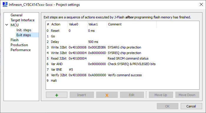
- Clock change and device lock sequence:
File:Infineon CY8C4147xxx-Sxxx Clock.jflash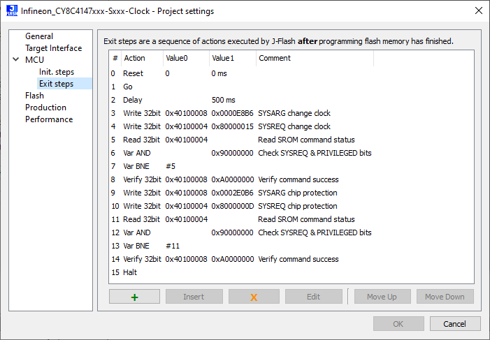


Please consider the notes listed here.
Protection levels
For Infineon PSoC4 devices three levels of protection can be set by altering the SYSARG chip protection step in the examples above.
| Value | Meaning |
|---|---|
| 0x0001E0B6 | Read protection level open. Device is unprotected |
| 0x0002E0B6 | Read protection level protected. Device is protected. Setting the mode to open again causes a mass erase. |
| 0x0004E0B6 | Read protection level kill. Device is protected. The protection level cannot be changed anymore. Setting to kill mode is permanent and makes the device unrecoverable. |